Silicon Wafer Sds
Our gold-coated silicon wafers use electron-beam lithography to form amorphous layers 50Å. Thickness 3 in.

Silicon Silicon Wafer Sigma Aldrich
Silicon Wafer Product Number.

. Silicon Carbide Wafer Product Number. Patterned silicon wafers Okmetic SSP DSP and SOI wafers with built-in patterns and buried. 647101 Silicon wafer single side polished N-type contains no dopant diam.
Ad Up To 150mm Semiconductor Wafers 3-Step Polishing For High Quality. All applicable American Elements. Safety Data Sheet SiliconSilicon Dioxide Wafer ACS Material LLC Version.
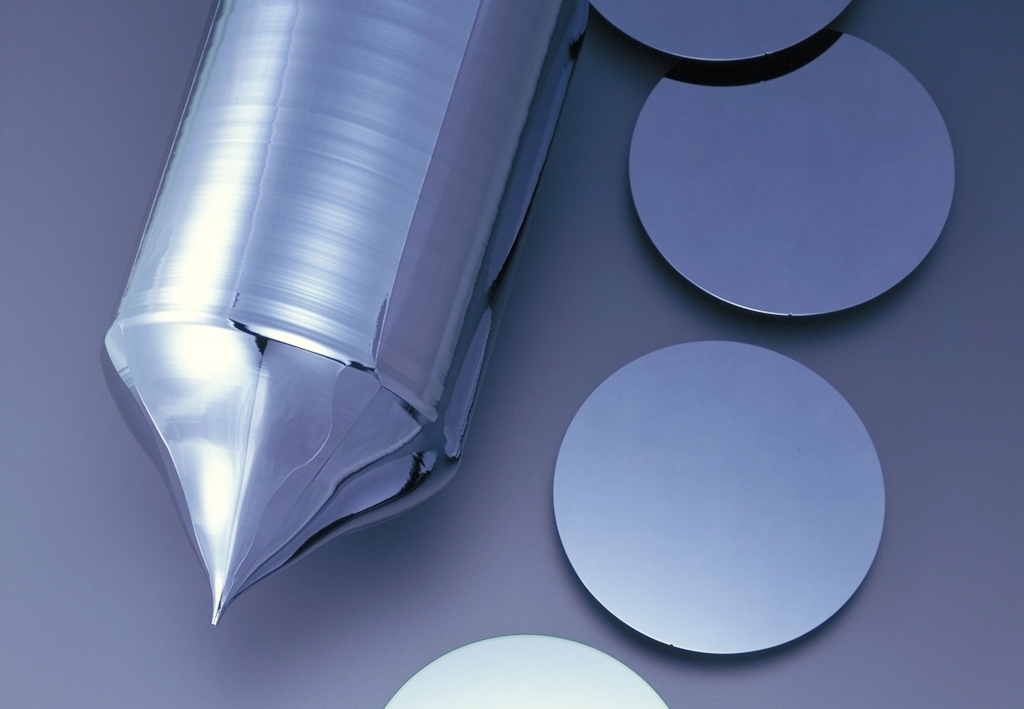
Wafer single side polished P-type contains boron as dopant diam. All applicable American Elements product. Our standard wafer diameters range from 254 mm 1 inch to 300 mm 118 inches in size.
SILICON WAFER SPECIFICATION We manufacture your own silicon wafers from 1 inch to 6. Ad Dynamic Process Group Specializes In Resizing Coring Wafers Of Various Types. Silicon Reference Standard Solution 1000ppm Certified Revision Date 24-December-2021.
Product Wafer MSDS Rev 30 06012022 Page 2 of 4 Revision date 06012022 MATERIAL. ACCIDENTAL RELEASE MEASURES 61. 14 rows Hyperpure silicon wafers are the basis for almost all semiconductor elements and.
Dynamic Process Group Will Work With You To Find The Best Solution For Your Specific Need. Silicon wafers are Non-flammable. Ad Find Over 15 Million Products at Grainger Today.
View and Print SDS About Silicon Wafer Boron-doped American Elements produces Boron. PRODUCT AND COMPANY IDENTIFICATION Product name. Fast Delivery Next Day Shipping on Most Orders and Access to 247 Knowledgeable Support.

Saliva And Serum Protein Adsorption On Chemically Modified Silica Surfaces J Lehnfeld Y Dukashin J Mark G D White S Wu V Katzur R Muller S Ruhl 2021
Semiconductor Chemistry Equipment Controls Technic Inc
Semiconductor Wafer Carrier Trays

Characterization Of Heterologously Expressed Fibril Filaments A Shape And Motility Determining Cytoskeletal Protein Of The Helical Bacterium Spiroplasma Biorxiv

Device Design Stage 2 Modified Microchannel Design Ppt Download
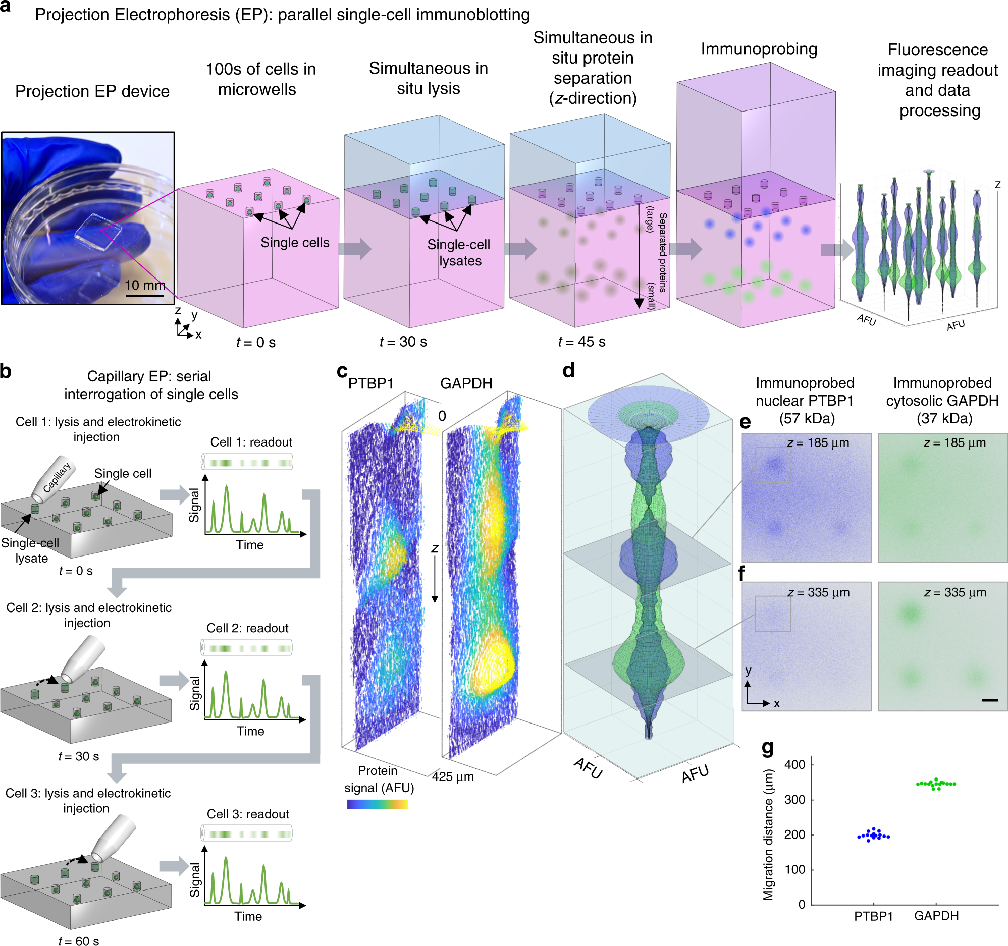
3d Projection Electrophoresis For Single Cell Immunoblotting Nature Communications

Effect Of The Surfactant Charge And Concentration On The Change In The Forces Between Two Charged Surfaces In Surfactant Solutions By A Liquid Flow Langmuir
Pdf Evaluation Of Hazardous Chemicals With Material Safety Data Sheet And By Products Of A Photoresist Used In The Semiconductor Manufacturing Industry

Cof Between The Glass Lens And Silicon Wafer Lubricated By 1 Mm Download Scientific Diagram
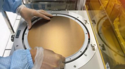
Silicon Wafers Semiconductor Materials Dept Electronics Materials Business Products Shin Etsu Chemical Co Ltd

Saliva And Serum Protein Adsorption On Chemically Modified Silica Surfaces J Lehnfeld Y Dukashin J Mark G D White S Wu V Katzur R Muller S Ruhl 2021

Pdf Electrical Characteristics Of Au N Si Ms Schottky Diodes Sds With And Without Different Rates Graphene Ca 1 9 Pr 0 1 Co 4 O X Doped Poly Vinyl Alcohol Interfacial Layer Prof Dr
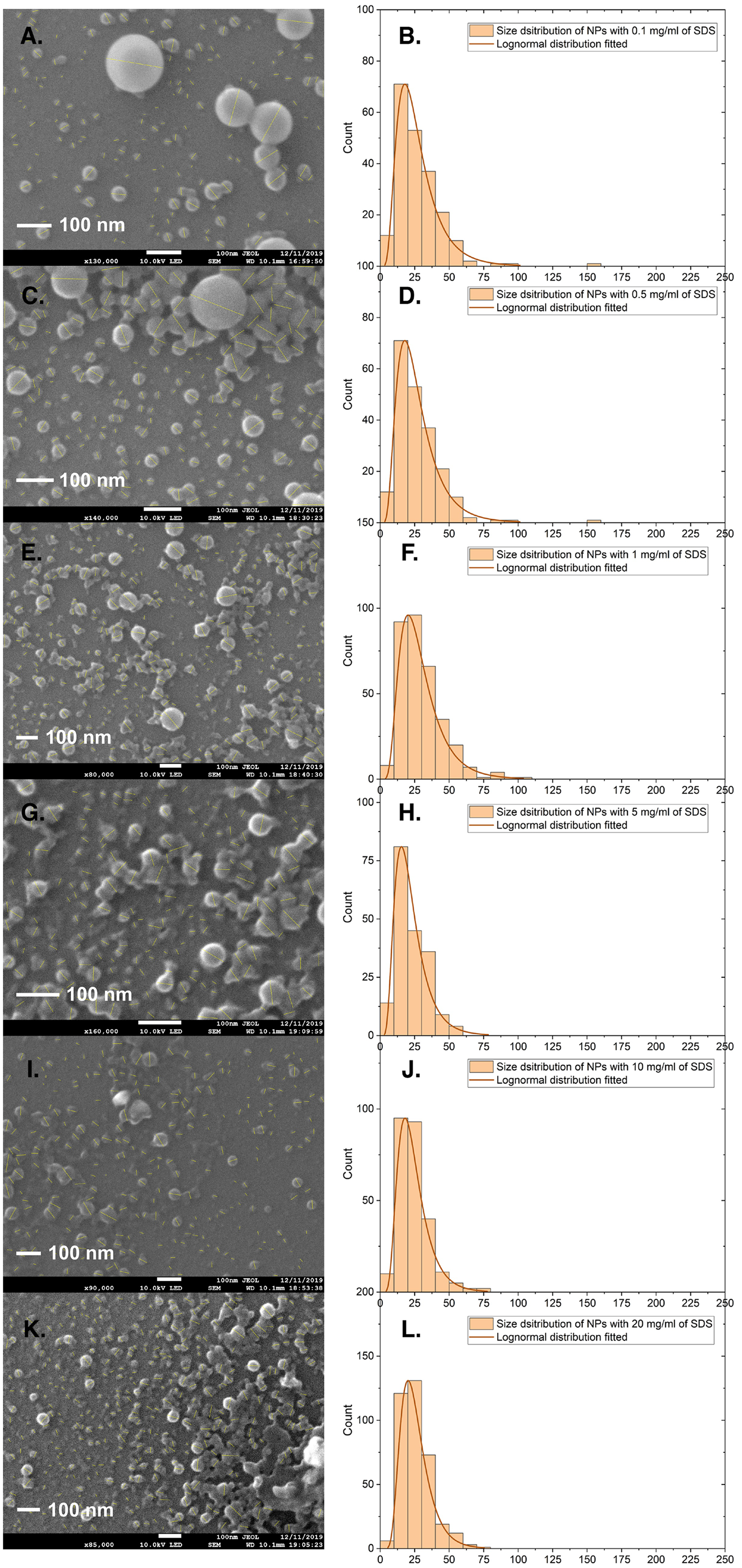
Synthesis Of Fluorescent Polystyrene Nanoparticles A Reproducible And Scalable Method Peerj

N Vs F Curve For Sds On Low Doped Hvpe Wafer Download Scientific Diagram

Pdf The Sds Process For Silicon Ribbon Growth Jorge Maia Alves Academia Edu

1 4 20 X 5 8 Phillips Flat Head Machine Screw Zinc Plated Hi Line Inc
What Scientific Research Are Silicon Wafers Used For